| McSwiggen & Associates |
 |
 |
 |
 |
 |
 |
 |
 |
/Applications/Characterization of Electronic Feedthroughs |

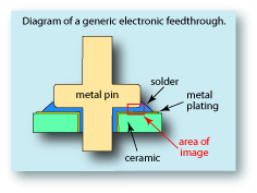
Electronic feedthroughs are used when a connector needs to be isolated from the surrounding housing through which it is passing. Typically a non-conductive ceramic is used to separate the two parts. The challenge is to produce a tight seal between very dissimilar materials, namely the metal conductor and the ceramic insulator. Below is a diagram of a typical feedthrough. The metal pin is the conductor which is passing through a ceramic insulator. The ceramic is usually plated or sputter-coated with a metal layer which will allow a metal solder to better adhere to the ceramic. The type of metal chosen for the metal layer is important because it will determine the adhesive characteristics. The type of solder used is even more important, as are its adhesive characteristics, melting temperature and resistance to corrosion – all must be considered.
|
 |
| The ability of metal alloys to resist corrosion may be seriously lessened if the alloy segregates into its separate components. Segregation can occur as a result of the temperature at which the alloy was heated, the rate it was cooled, or an interaction with other metal components. Electron microprobes are ideal for characterizing the solder or weld connecting the conductor of a feedthrough to its ceramic insulator. Below is a backscattered electron image of a portion of a feedthrough showing the solder join between the metal pin and aluminum oxide insulator. The structure is complex because of the various metal-plated layers required to produce a stable, strong bond between the various components. But the image also shows that segregation has occurred, possibly reducing the likelihood that the material will behave as originally designed. |
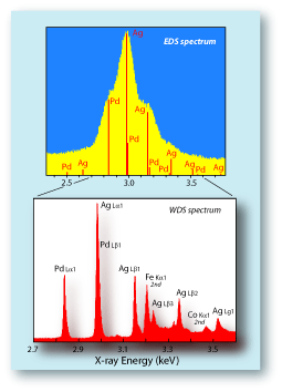
| Above, right, shows portions of an energy dispersive spectrometer (EDS) spectrum and a wavelength dispersive spectrometer (WDS) spectrum collected on the join material (solder) to identify the elements present. One can see that the EDS spectrum cannot resolve the individual X-ray lines of Ag and Pd. All of the lines are displayed as one single peak. Therefore it would be very difficult to, for example, map the distribution of the Pd and Ag, because they could not be differentiated. On a WDS system, though, the X-ray lines are separate enough to allow them to be measured independently for either quantitative or map analyses. | 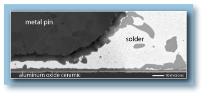 |
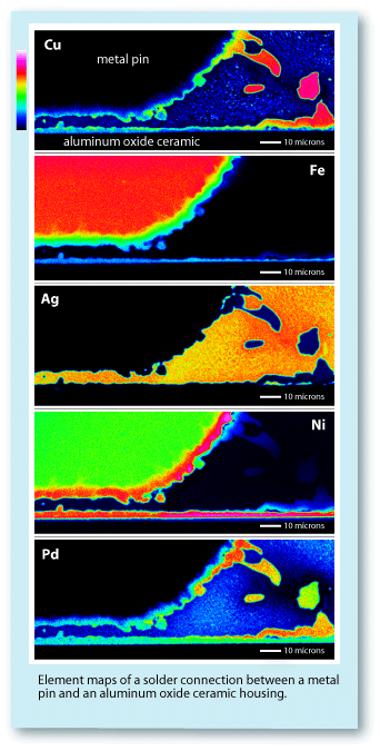 |
To the right are element maps collected using wavelength dispersive spectrometers
(WDS) of the same area displayed in the
previous backscattered electron image.
Each map shows the distribution of a single
element across the mapped area. Those
portions of the maps occupied by orange
and red have a high abundance of that
particular element. Those areas colored
blue or black have a low or no concentration
of that element. These maps are qualitative
in nature but can be quantified using standard quantitative analysis methods. The WD spectrometers made it possible to distinguish the Ag from the Pd on the maps, which can be seen to have segregated separate areas. Also because of the higher count rates of the WD spectrometers, these maps could be collected in 1/10 the time required by the ED spectrometer.The significance of these element maps is that they show how the feedthrough was constructed. One can immediately see the relative differences between the pin, the solder, and the metal-plated edge of the ceramic insulator. The element maps show that both the metal pin and the ceramic insulator. were metal plated or sputter coated with at least two layers of different Cu, Ni, Fe, and Pd alloys, and that the solder is a Cu-Ag-Pd alloy which has segregated into two primary phases, a high-Ag phase and a high-Pd-Cu phase.Element maps such as these can be used for quality control purposes or for competitive evaluations, since they clearly detail the device's characteristics. The points that would be of interest to focus on would include:
|